Knowledge Center
AO3401 PNP Mosfet 4A 30V

Intro #
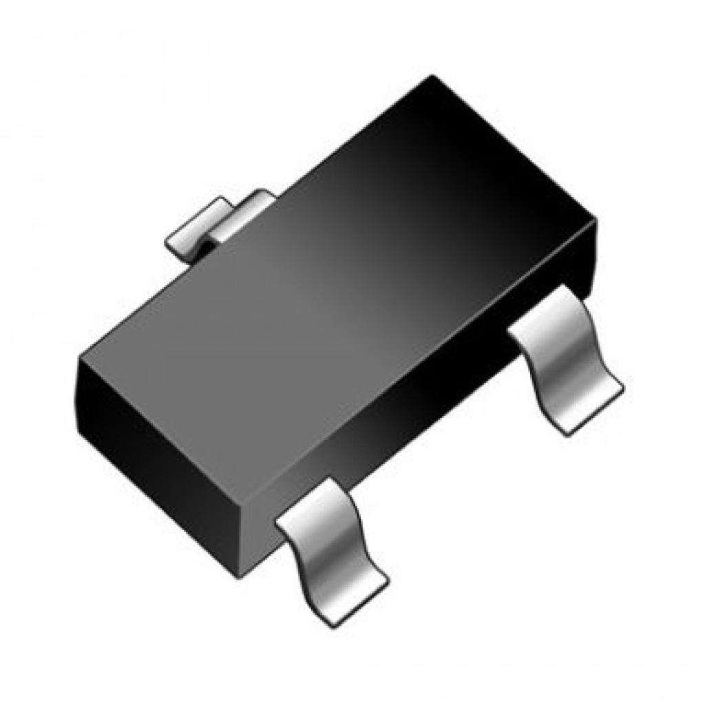
AO3401 is a field effect transistor (FET), belonging to voltage-controlled semiconductor devices. AO3401 has the advantages of high input resistance, low noise, low power consumption, no secondary breakdown, wide safe working area, as well as low temperature and radiation effects. AO3401 is especially suitable for high sensitivity and low noise circuitry. The AO3401 utilizes advanced trench technology to provide excellent RDS(ON), low gate charge and operation at gate voltages as low as 2.5V. The device is suitable for use as a load switch or is used in pulse width modulation applications. Standard product AO3401 is lead free (RoHS and Sony 259 compliant).
The AO3401 leads out 3 pins in the SOT-23 package and is a low power FET. The pulsed drain current (IDM) of AO3401 is 30A, the zero gate voltage drain current (IDSS) is 1uA. Its temperature resistance range is -55~150 degrees Celsiusn during operation. The gate-source voltage (VGS) of the AO3401 is ±12V. AO3401 SMD package series feature a body length of 1.7mm, plus pin length of 2.95mm, width of 3.1mm, height of 1.3mm, and pin spacing of 1.9mm.
The AO3401 is especially suitable for high sensitivity and low noise circuits and can be used as a load switch or in pulse width modulation applications.
Specification #
Operating Temperature: -55°C~150°C TJ
Power Dissipation-Max: 1.4W Ta
Operating Mode: ENHANCEMENT MODE
FET Type: P-Channel
Transistor Application: SWITCHING
Rds On (Max) @ Id, Vgs: 50m Ω @ 4A, 10V
Vgs(th) (Max) @ Id: 1.3V @ 250μA
Input Capacitance (Ciss) (Max) @ Vds: 645pF @ 15V
Current – Continuous Drain (Id) @ 25°C: 4A Ta
Gate Charge (Qg) (Max) @ Vgs: 14nC @ 10V
Drain to Source Voltage (Vdss): 30V
Drive Voltage (Max Rds On,Min Rds On): 2.5V 10V
Vgs (Max): ±12V
Drain Current-Max (Abs) (ID): 4A
Drain-source On Resistance-Max: 0.05Ohm
DS Breakdown Voltage-Min: 30V
Datasheet #
AO3401 control 3.3V 5V power supply circuit #
AO3401 is cheap and low cost for small voltage circuit control

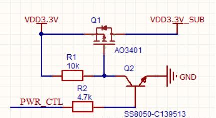
The working principle of the circuit is:
PWR_CTL is connected to the GPIO port of the microcontroller and needs to be pulled up internally or externally.
When PWR_CTL is high level: the transistor SS8050 is turned on at this time, the gate (G) of Q1 is equivalent to grounding, there is a negative voltage between the gate (G) and the source (S), the MOS tube is turned on, and the drain (D) ) has a 3.3V output.
When PWR_CTL is low level: the transistor SS8050 is not turned on at this time, there is no voltage difference between the gate and the source stage of the MOS tube, the MOS tube is turned off, and there is no voltage output.
The application of field effect transistor AO3401 in the circuit

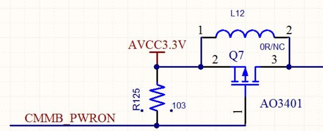
This is a circuit that controls the power on and off, AO3401 is an enhancement mode PMOS. Simply put, Q7 turns on when Vgs (that is, the voltage between 1-2 of Q7) is negative. For AO3401, the full turn-on voltage is around -10V, but -3.3V can basically be turned on, but the impedance is slightly larger (about 100 milliohms). For the specific on-resistance under different Vgs voltage, please refer to the AO3401 manual. For the circuit in the figure, when CMMB_PWRON is greater than or equal to 3.3V, the AO3401 is off, and the back-end circuit is not powered. When CMMB_PWRON is 0V, AO3401 is turned on and the back-end circuit is powered. When using this switch, L12 should not be soldered, otherwise this circuit is meaningless.
Source #
https://www.easybom.com/blog/a/an-introduction-to-field-effect-transistor-fet-ao3401


